Finite State Machine Divider (FSDM)
The purpose of this project was to research and design digital dividers, implement Finite State Machines that can process data, and create a complex digital system using System Verilog and a Basys3 FPGA.
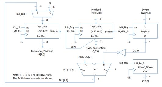
This Finite State Machine (FSM) will serve to perform the division operation on 2 byte sized binary numbers using principles of long division. This system will make use of shift registers, state machines, complex mathematical operations, and the 7-segment display available on the Basys3. The 16 dip switches on the Basys3 will serve as the inputs to the system with bits 15-8 as the dividend and 7-0 as the divisor. The system will perform this operation and display the remainder in decimal on the 7 segment display, while the 16 on board LEDs will show the remainder in base 2.
A high level schematic of the system can be viewed here.
Circuit Diagram of System
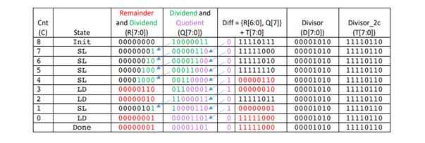
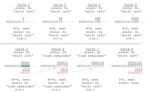
The algorithm used to accomplish this binary division is simple long division. The following table and operation step through figure shows an example of this operation with 10000011 as the dividend and 00001010 as the divisor. This will help visualize how the registers shift throughout the operation.
State Machine Step Table
State Machine Step Visualization
Finally, the FSM that was designed for this purpose was a Mealy Machine, and it can be visualized by the graph below. Code, in system verilog, will also be provided below instead of on GitHub as this project was not pushed to any repositories. I apologize for the blurriness of some screenshots, these are all that I have.
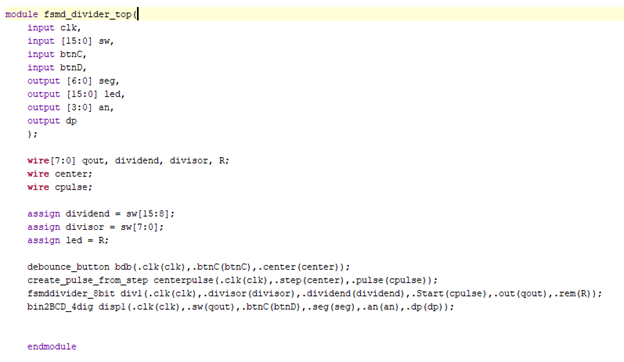
FSM Top Module
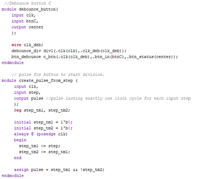
Button Debounce and Pulse Generation
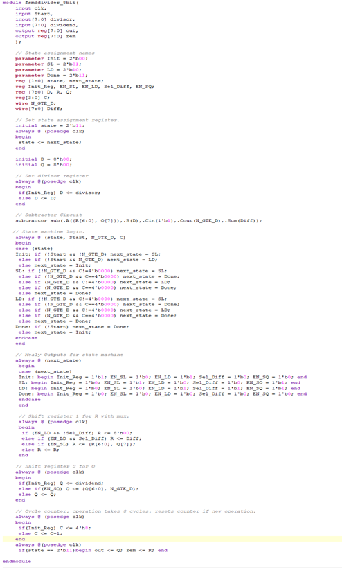
State Machine Divider
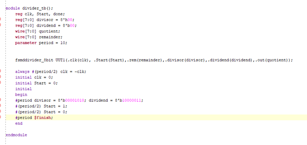
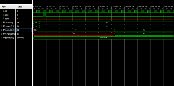
A test bench was written to ensure proper function of the machine. The code for the bench is below, along with a time graph demonstrating proper and expected results.
Test Bench Code
Test Bench Timing Graph
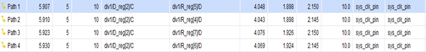
Finally, looking at figure below, we can see that our worst negative slack is 5.907. This is the slowest path in our design, and it represents the amount of time left in our current clock period. This means we can theoretically increase the clock frequency to 1 / (10ns - 5.907ns). This would give us an appoximate maximum frequency of about 244MHz. Knowing that this operation takes 8 cycles I was tempted to conclude that the division operation takes 8 clock cycles. This may be the case for the division operation itself; however, to receive output from the module it requires more. Stepping through the program and watching the timing graph, I was able to observe that this design took about 11 positive clock edges to fully complete and send the output back to the top module.
Timing Evaluation